The news that Samsung Electronics and SK Hynix are reviewing investments in South Korea’s Honam region foreshadows a massive butterfly effect, intertwining the reorganization of domestic and international supply chains with the fierce battle for hegemony in the artificial intelligence (AI) semiconductor market.
We analyze the reality of Samsung Electronics’ push for a 100% humanoid manufacturing facility (AI-driven factory) and look into the future outlook of global AI semiconductor investments connecting Taiwan, South Korea, and ASEAN.
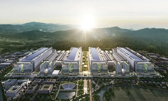
1. Samsung Electronics’ 100% Humanoid Manufacturing Facility Implementation Process
Samsung Electronics is aiming for a complete transition by 2030 to its “AI Driven Factory.” The deployment of humanoid robots is being implemented phase by phase across all manufacturing stages—not just in the front-end processes (Fab) like chip design and wafer fabrication, but also in material receiving, logistics, precision assembly, and back-end processes (packaging and testing).
- Connection to Honam Investment (Highly Likely to be a Packaging Process): As analyzed by Ahn Ki-hyun, Executive Director of the Korea Semiconductor Industry Association, and other industry experts, the newly planned facility under review for the Honam region is highly likely to be a back-end Advanced Packaging factory rather than a fabrication plant (Fab) that inherently demands massive amounts of water and power.
- Automation and Robotization of the Packaging Process: Packaging is a precision assembly stage where round wafers are diced into individual chips and encased in protective materials. Historically, this sector has relied heavily on manual labor with a higher proportion of production workers than engineers. To achieve complete automation of this back-end fab, Samsung Electronics is actively testing humanoid manufacturing robots, operating bots, and assembly bots integrated with Overhead Hoist Transport (OHT) wafer transfer systems.
- Risk Management: This strategy prioritizes deploying humanoid robots in infrastructure, environmental, and safety sectors exposed to high temperatures, intense noise, or hazardous substances. This approach aims to maximize 24-hour operational efficiency while elevating workplace safety.
2. Global AI Semiconductor Investment Outlook (Taiwan · South Korea · ASEAN)
Current global semiconductor investments are shifting away from a single-hub concentration, restructuring into a hybrid network architecture to ensure stable supply chains and diversify geopolitical risks.
① Lock-in of Taiwan-Centric Fine Node Processes and Foundries (NVIDIA-TSMC)
NVIDIA continues its heavy, concentrated investment in Taiwan, relying entirely on TSMC’s advanced foundry (contract manufacturing) processes and CoWoS (Chip-on-Wafer-on-Substrate) packaging technology. While this solidifies the solidarity of the ultra-fine node ecosystem, it carries a critical vulnerability regarding geopolitical risks (cross-strait relations).
② South Korea’s Convergence Supply Chain and Regional Production Line Synergy (Samsung · SK · Doosan)
To counter these challenges, South Korea is employing a strategy that links the Honam region with the Yongin Semiconductor Mega Cluster (Memory, HBM, Foundry) acting as the main hub.
- HBM Supply Chain and Honam’s RE100 Synergy: Amid mounting pressure from global big tech companies to comply with RE100 mandates, Honam’s abundant renewable energy infrastructure serves as an excellent alternative for advanced packaging (HBM stacking and packaging) facilities where clean electricity is vital.
- Physical AI Collaboration (Doosan Robotics, etc.): The push toward production line automation and AI-driven factories by Samsung and SK is vitalizing a collaborative ecosystem with leading domestic robotics companies like Doosan Robotics. Data accumulation for semiconductor-line-tailored collaborative robots and Physical AI (AI for robot control) is taking place earliest in Korea, completing a “Semiconductor-Robotics” convergence ecosystem through balanced regional investment.
③ Integration with ASEAN’s AI Semiconductor Back-end/Testing Network
Core dies and HBM produced in South Korea and Taiwan are transferred to concentrated Outsourced Semiconductor Assembly and Test (OSAT) hubs in the ASEAN region—including Malaysia, Vietnam, and Singapore—to form a network for final modularization. Benefiting from lower labor costs and relative freedom from US-China geopolitical friction, ASEAN is rapidly emerging as a critical hub for lower-tier packaging and the final consumption of AI semiconductors, aligning with the booming construction of Southeast Asian data centers by big tech giants.
Comprehensive Outlook: Future global investments will form a sophisticated division of labor structured as “Taiwan (Advanced Foundry) → South Korea (HBM and Eco-friendly/Robot-based Autonomous Packaging Hub) → ASEAN (Final Assembly & Data Center Integration).” South Korea’s core competitiveness will rest on securing an independent and secure automated packaging value chain by weaving together Honam’s renewable energy with domestic robotics technology.
Leave a Reply